|
Context of project A long standing technological challenge is the integration of high optical quality III-V semiconductor nanostructures with the mainstream of electronic industry based on Silicon. Such integration may allow the development of single photon sources, light mediated quantum information and novel photovoltaic modules. III-V nanowires on Silicon ref: [1] www.nature.com/articles/s41467-019-08807-9 Our work We realize the growth of self-catalyzed core–shell GaAs/GaAsP nanowires (NWs) on Si substrates using molecular-beam epitaxy. Transmission electron microscopy of single GaAs/GaAsP NWs demonstrates their high crystal quality and shows domination of the GaAs zinc-blende phase. Using continuous-wave and time-resolved photoluminescence (PL), we make a detailed comparison with uncapped GaAs NWs to emphasize the effect of the GaAsP capping in suppressing the nonradiative surface states. Significant PL enhancement in the core–shell structures exceeding 3 orders of magnitude at 10 K is observed; in uncapped NWs PL is quenched at 60 K, whereas single core–shell GaAs/GaAsP structures exhibit bright emission even at room temperature. From analysis of the PL temperature dependence in both types of NW we are able to determine the main carrier escape mechanisms leading to the PL quench. Read more: Effect of a GaAsP shell on the optical properties of self-catalyzed GaAs nanowires grown on silicon O.D.D. Couto Jr, D. Sercombe, J. Puebla, L. Otubo, I.J. Luxmoore, M. Sich, T.J. Elliott, E.A. Chekhovich, L.R. Wilson, M.S. Skolnick, H.Y. Liu, A.I. Tartakovskii Nano letters 12 (10), 5269-5274 (2012) https://pubs.acs.org/doi/10.1021/nl302490y arXiv: arxiv.org/abs/1206.4857 Personal contribution: Nanowire sample mapping and high resolution microscopy 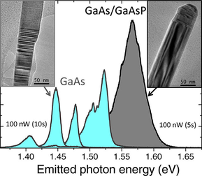
0 Comments
Leave a Reply. |
Jorge PueblaResearch Scientist Archives
October 2020
Categories |
 RSS Feed
